RTL93xx SoCs
All information in this page is curated from the SDK sources (which are known to contain errors) or trial and error. Do not assume anything on this page is perfectly correct!
RTL930x SoCs
All SoCs in this series have a 34Kc MIPS core.
Clock tree
The picture below draws the clock tree as per documentation. What is unclear and obviously missing, is the SRAM PLL, which we do find in the sdk.
While the documentation speaks of an optional 156.25 Mhz Clock, no pintout seems to match this.
Clock Controller
The Flattened Clock generator (as the SDK calls it).
Bus tree
Peripherial Map
The realtek memory map is like like spaghetti, where registers are all over the place. Some things are almost logical, but not when looking at Linux based frameworks. The following table gives an overview of where to expect certain register:bits for a specific peripheral.
| Peripherial | Main space | PinController? | Notes |
|---|---|---|---|
| QSPI-NOR Controller | Peripherial | NA | |
| SPI_SLV Controller | SwitchCore | ||
| SPI Controller | SwitchCore | ||
| I2C Controller 0 | SwitchCore | SwitchCore | |
| I2C Controller 1 | SwitchCore | SwitchCore | |
| UART 0 | Peripherial | NA | |
| UART 1 | Peripherial | SwitchCore | |
| JTAG | |||
| Reset Controller | SwitchCore | ||
| PAD Controller | SwitchCore | ||
| GPIO Controller | |||
| Extra GPIO Controller | SwitchCore | SwitchCore | |
| Led Controller | SwitchCore | ||
| Extra LED Controller | SwitchCore | SwitchCore | |
| MDIO Controller | SwitchCore |
Interrupt Map
Interrupts are a bit more complex with both an interrupt and a routing component. See SoC interrupt controller for details.
| Interrupt source | IRQ | VPE0 IRQ destination (SDK) | VPE1 IRQ destination (SDK) | Notes |
|---|---|---|---|---|
| DELAY2 | 2 | |||
| DELAY3 | 3 | |||
| DELAY4 | 4 | |||
| WDT_IP1 | 5 | 4 | ||
| WDT_IP2 | 6 | 4 | Only listed as ISR | |
| TIMER0 | 7 | 5 | ||
| TIMER1 | 8 | 5 | ||
| TIMER2 | 9 | |||
| TIMER3 | 10 | |||
| TIMER4 | 11 | |||
| Lexra Bus Traffic Generator/GDMA | 12 | |||
| GPIO0 (ABCD) | 13 | 1 | ||
| Reserved | 14 | |||
| SLXTO/LXSTO | 15 | |||
| HLXTO/LXMTO | 16 | |||
| OCPTO | 17 | |||
| Reserved | 18 | |||
| SPI_NAND | 19 | |||
| ECC (Hashing) | 20 | |||
| Reserved | 21 | |||
| SECURITY (Crypto) | 22 | |||
| SWCORE | 23 | 2 | ||
| NIC | 24 | 3 | ||
| Reserved | 25 | |||
| Reserved | 26 | |||
| Reserved | 27 | |||
| USB_H2 | 28 | 2 | ||
| Reserved | 29 | |||
| UART0 | 30 | 1 | ||
| UART1 | 31 | 0 |
Memory Map
The memory map addresses are obtained from a combination of the devicetree and the memory_map header
Phsyical map
| Bus | Address start | Address end | size | Function | Note |
|---|---|---|---|---|---|
| OCP* | 0x0000_0000 | 0x0800_0000 | 0x0800_0000 | DDR Memory access | 1Gbit (128MiB) max RAM as per datasheet, RTL8197F datasheet proclaims 256MiB address space |
| OCP* | 0x1400_0000 | 0x17FF_FFFF | 0x0400_0000 | QSPI FLash memory mapped | 512Mbit (64MBiB), RTL8197F proclaims 128MiB starting at 0x10000000 |
| Lexra Peripherial Bus | 0x1800_0000 | 0x1820_0000 | 0x0020_0000 | SoC Peripherial register space | |
| Lexra LX0 | 0x1B00_0000 | 0x1D00_0000 | 0x0200_0000 | SwitchCore | Register details |
| OCP* | 0x1F00_0000 | 0x1F01_0000 | 0x0001_0000 | SRAM | Used by BootROM, free for other uses by kernel (Header states 128KB, doc states 64KB |
| OCP* | 0x1FB0_0000 | - | - | RTC? | Mentioned in the RTL8197 SDK … |
| OCP* | 0x1FC0_0000 | 0x1FD0_0000 | 0x0010_0000 | CPU Boot ROM | Boot code executed by CPU to load SPL from Flash ? Address from RTL8197F Datasheet, so could be wrong. We should see if it is actually there and if we can extract it! |
| OCP* | 0x1FD0_0000 | 0x1FE0_0000 | 0x0010_0000 | ROM | Mini OS that configures the switch based on EEPROM ? Address from RTL8197F Datasheet, so could be wrong. We should see if it is actually there and if we can extract it! |
OCP* Directly connected to the CPU address bus
SoC Peripherial map
The SoC Peripherial map and register map. To read from U-Boot an offset of `0xb8000000` where linux accesses the uncached `0x18000000` is required to address registers via kseg1.
| Address start | Address end | size | Function |
|---|---|---|---|
| 0x000000 | 0x000007 | 0x000008 | SoC ID Registers |
| 0x000008 | 0x00004b | 0x000048 | Lexra Bus Controller |
| 0x000100 | 0x000103 | 0x000004 | PIN Status |
| 0x000104 | 0x000113 | 0x000010 | PAD Controller |
| 0x000114 | 0x000143 | 0x000030 | DDR IO Control |
| 0x000200 | 0x000233 | 0x000033 | CLK Controller |
| 0x000388 | 0x0005ff | 0x000278 | CMU Controller |
| 0x000400 | 0x0004ff | 0x000100 | BIST (Built In Self Test) Controller |
| 0x000500 | 0x0005ff | 0x000100 | USB PHY (ANA) Controller (UPCR) |
| 0x000600 | 0x000603 | 0x000004 | IP Enable Controller |
| 0x000608 | 0x00060b | 0x000004 | DLL Controller |
| 0x00060c | 0x00060f | 0x000004 | SYS MISC Controller |
| 0x000610 | 0x000617 | 0x000008 | DLL ANA Controller |
| 0x000618 | 0x00063b | 0x000024 | Speed Sensor Controller |
| 0x00063c | 0x00063f | 0x000004 | New IP Enable Controller |
| 0x700 efuses? | |||
| 0x001000 | 0x0010ff | 0x000100 | Memory controller (includes multiple items, inc. memory controller versioning) |
| 0x001200 | 0x00121b | 0x00001c | SPI0 Controller |
| 0x001300 | 0x001307 | 0x000008 | UMSAR / UNMAP / UMSAR/UMSSR 0 |
| 0x001310 | 0x001317 | 0x000008 | UMSAR / UNMAP / UMSAR/UMSSR 1 |
| 0x001320 | 0x001327 | 0x000008 | UMSAR / UNMAP / UMSAR/UMSSR 2 |
| 0x001330 | 0x001337 | 0x000008 | UMSAR / UNMAP / UMSAR/UMSSR 3 |
| 0x001500 | 0x0015df | 0x0000e0 | DDR PHY Memory Controller |
| 0x001600 | 0x001613 | 0x000014 | Mem Cache Controller |
| 0x002000 | 0x002017 | 0x000018 | UART0 |
| 0x002100 | 0x002117 | 0x000018 | UART1 |
| 0x003000 | 0x003023 | 0x000024 | Interrupt controller |
| 0x003080 | 0x003093 | 0x000014 | Delayed Interrupt Controller |
| 0x003200 | 0x00300f | 0x000010 | Timer0 |
| 0x003210 | 0x00301f | 0x000010 | Timer1 |
| 0x003220 | 0x00302f | 0x000010 | Timer2 |
| 0x003230 | 0x00303f | 0x000010 | Timer3 |
| 0x003240 | 0x00304f | 0x000010 | Timer4 |
| 0x003250 | 0x00325f | 0x000010 | Timer5 |
| 0x003260 | 0x00326b | 0x00000c | Watchdog Timer |
| 0x003300 | 0x00331b | 0x00001c | GPIO0 Controller (ABCD) |
| 0x00331c | 0x003337 | 0x00001c | GPIO1 Controller (EFGH) |
| 0x003338 | 0x00333f | 0x000008 | GPIO0 affinity |
| 0x003340 | 0x003348 | 0x000008 | GPIO1 affinity |
| 0x004000 | 0x0040fb | 0x0000fc | SRAM Controller |
| 0x004080 | 0x00408b | 0x00000c | ROM Controller |
| 0x004090 | 0x00409b | 0x00000c | SRAM Misc Controller |
| 0x004200 | 0x004233 | 0x000034 | DDR PHY Memory Controller |
| 0x005100 | 0x00526c | 0x00016c | OB to MONT |
| 0x005200 | 0x00520b | 0x00000c | Lexra bus to MONT |
| 0x00a000 | 0x00a23b | 0x00023c | Lexra Bus 1 Traffic Generator |
| 0x00c000 | 0x00c00b | 0x00000c | IP Sec Crypto engine (generic crypto engine?) |
| 0x018000 | 0x01823b | 0x00023c | Lexra Bus 2 Traffic Generator |
| 0x01a400 | 0x01a443 | 0x000044 | SPI NAND flash Controller |
| 0x01a600 | 0x01a653 | 0x000054 | ECC Controller (Error Correcting Code (BCH) CODEC) |
| 0x020000 | 0x020000 | 0x000100 | USB OHCI Controller (based of rtl819x datasheet) |
| 0x021000 | 0x0210a4 | 0x0000a4 | USB EHCI Controller (rtk_gen1-ehci) |
| 0x0210a4 | 0x021xxx | 0x000xxx | EHCI UTMI |
| 0x140200 | 0x1402xx | 0x0000xx | USB-PHY Frequency/Ext CFG? |
| 0x144000 | 0x14423b | 0x00023c | Lexra Bus 0 Traffic Generator |
PIN Status 0 0x100
Could be likely the strapping pins or configuration registers
| BITs | Name | Description |
|---|---|---|
| 31:20 | - | Must be zero |
| 19:18 | DRAM_TYPE | DDR1/DDR2/DDR3? |
| 17:16 | BOOT_UP_TYPE | SPI/Nor boot type? |
| 15 | enctrlch | |
| 14:13 | CS1_MUX_SEL | Chip Select 1 Mux select |
| 12 | - | Must be zero |
| 11 | - | Unused |
| 10 | - | Must be zero |
| 9 | spictrl | SPI control? |
| 8 | flshcfg | Flash Configuration? |
| 7 | SPI_FLASH_4B_EN | 3 or 4 byte SPI address mode? |
| 6 | pin_cksel | Pin Clock Select? |
| 5 | testmode/SCAN_MODE | Must be zero |
| 4 | SPEED_UP | |
| 3:0 | cpmode | Must be zero |
PIN Status 1 0x104
Could be likely the strapping pins
| BITs | Name | Description |
|---|---|---|
| 31:3 | - | Must be zero |
| 2 | spifben | SPI Flash Enable? |
| 1:0 | sdckg | ? |
Longan
RTL930x
SoC series with condename "Longan".
Common features:
- Single core MIPS 34Kc with dual threading @ 800MHz
- 1.5MB of packet buffer
| Model number | MODEL_NAME_INFO | Ports | Comment |
|---|---|---|---|
| 9301 (Datasheet) | 24x GE, 4x 10GE | 4 pairs of 8Gbps SerDes allows stacking additional 9301 for 48x GE, 4x 10GE, 128 GBit switch cap | |
| 9302A | 0x93020810 | 12 x 2.5G | 60 GBit switch cap |
| 9302B | 0x93021010 | 8 x 2.5G | 40 GBit switch cap |
| 9302C | 0x93021810 | 16 x 2.5G | 80 GBit switch cap |
| 9302D | 0x93022010 | 24 x 2.5G | 120 GBit switch cap |
| 9302A | 0x93020800 | 8x GE, 12x 2.5GE, 4x 10GE | No emb. PHY, 156 Gbit switch cap |
| 9302B | 0x93021000 | 16x GE, 8x 2.5GE, 4x 10GE | No emb. PHY, 152 GBit switch cap |
| 9302C | 0x93021800 | 16x 2.5GE, 4x 10GE | No emb. PHY, 160 GBit switch cap |
| 9302D | 0x93022000 | 24x 2.5GE, 2x 10GE | No emb. PHY, 160 GBit switch cap |
| 9302F | 0x93023001 | ||
| 9303 (Datasheet) | 0x93030001 | 8× 10G | 160Gb/s switching capacity |
9301
As we only have the datasheet for the RTL9301, this is the only hard evidence for the device due to pinouts that we know. Also important to note, that Only SserDes 2, 4, 6 and 8 have differential clock-pairs. There's also 4 single pole clock outputs.
| SerDes | Switch Ports | MII name | Notes |
|---|---|---|---|
| 0 | 0-3 | QSGMII | 4Gbit, commonly combined with sds1 to form dual QSGMII to drive octal gbit PHY's |
| 1 | 4-7 | QSGMII | 4Gbit, commonly combined with sds0 to form dual QSGMII to drive octal gbit PHY's |
| 2 | 8-15 | XSGMII | 10Gbit for use with octal 1Gbit PHY, or quad 2.5G PHY or dual 5G PHY or one 1/2.5/5/10 copper PHY |
| 3 | 16-23 | XSGMII | 10Gbit for use with octal 1Gbit PHY, or quad 2.5G PHY or dual 5G PHY or one 1/2.5/5/10 copper PHY |
| 4 | 24 | 10GBase-R | 10/1Gbit for use with 1/10 SFP+ PHY's |
| 5 | x | x | SerDes 5 is unavilable in single SoC layouts |
| 6 | 25 | 10GBase-R | 10/1Gbit for use with 1/10 SFP+ PHY's |
| 7 | 28 | SGMII | 1Gbit for use with CPU interface (via Table 7) |
| 8 | 26 | 10GBase-R | 10/1Gbit for use with 1/10 SFP+ PHY's |
| 9 | 27 | 10GBase-R | 10/1Gbit for use with 1/10 SFP+ PHY's |
The 9301 can also be configured in cascading mode, where the master or slave, uses the following serdes layout
| SerDes | Switch Ports | MII name | Notes |
|---|---|---|---|
| 0 | 0-3 | QSGMII | 4Gbit, commonly combined with sds1 to form dual QSGMII to drive octal gbit PHY's |
| 1 | 4-7 | QSGMII | 4Gbit, commonly combined with sds0 to form dual QSGMII to drive octal gbit PHY's |
| 2 | 8-15 | XSGMII | 10Gbit for use with octal 1Gbit PHY, or quad 2.5G PHY or dual 5G PHY or one 1/2.5/5/10 copper PHY |
| 3 | 16-23 | XSGMII | 10Gbit for use with octal 1Gbit PHY, or quad 2.5G PHY or dual 5G PHY or one 1/2.5/5/10 copper PHY |
| 4 | 24 | RSXGMII | RXAUI+ interface to connect to cascaded switch (combined with sds5) |
| 5 | 24 | RSXGMII | RXAUI+ interface to connect to cascaded switch (combined with sds4) |
| 6 | 25 | RSXGMII | RXAUI+ interface to connect to cascaded switch (combined with sds7) |
| 7 | 25 | RSXGMII | RXAUI+ interface to connect to cascaded switch (combined with sds6) |
| 8 | 26 | 10GBase-R | 10Gbit for use with 1/10 SFP+ PHY's |
| 9 | 27 | 10GBase-R | 10Gbit for use with 1/10 SFP+ PHY's |
9302
As we have no datasheet for the RTL9302, this is based from code and 'how it seems to work', so some salt grains are needed here. Some unknowns are, we have 152 Gbit, or 76 GBit FD, and know that at most, we have to do 16 * 1GE, 8 * 2.5GE and 4 * 10GE. We also know that XGS1210/1250 use the last 4 serdes for those non-GE ports, and sds2 for an octal PHY using port 0 - 7. We also know we can't change port and serdes numbers, they are matched. It thus seems likely, considering the 9301 and minimal changes, that sds0 and 1 have been 'repurposed' for quad 2.5G serdes (10G), as we need to put 8x2.5 somewhere, again, can't change port numbers. We also know, that sds6-9 are single port serdeses, so the following table seems possible.
| SerDes | Switch Ports | MII name | Notes |
|---|---|---|---|
| 0 | x | No data available for this serdes | |
| 1 | x | No data available for this serdes | |
| 2 | 0-7 | XSGMII | 10Gbit for use with octal 1Gbit PHY, or quad 2.5G PHY or dual 5G PHY or one 1/2.5/5/10 copper PHY |
| 3 | 8-15? | XSGMII? | Unknown function of serdes Likely |
| 4 | 16-19? | ? | Unknown function of serdes Quad 2.5G? |
| 5 | 20-23? | ? | Unknown function of serdes Quad 2.5G? |
| 6 | 24 | 10GBase-R/XSGMII | 10/1Gbit for use with 1/10 SFP+ PHY's for use with octal 1Gbit PHY, or quad 2.5G PHY or dual 5G PHY or one 1/2.5/5/10 copper PHY? |
| 7 | 25 | 10GBase-R/XSGMII | 10/1Gbit for use with 1/10 SFP+ PHY's for use with octal 1Gbit PHY, or quad 2.5G PHY or dual 5G PHY or one 1/2.5/5/10 copper PHY? |
| 8 | 26 | 10GBase-R/XSGMII | 10/1Gbit for use with 1/10 SFP+ PHY's for use with octal 1Gbit PHY, or quad 2.5G PHY or dual 5G PHY or one 1/2.5/5/10 copper PHY? |
| 9 | 27 | 10GBase-R/XSGMII | 10/1Gbit for use with 1/10 SFP+ PHY's for use with octal 1Gbit PHY, or quad 2.5G PHY or dual 5G PHY or one 1/2.5/5/10 copper PHY? |
9303
As we have no datasheet for the RTL9303, this is based from code and 'how it seems to work', so some salt grains are needed here.
| SerDes | Switch Ports | MII name | Notes |
|---|---|---|---|
| 0 | x | QSGMII? | No data available for this serdes |
| 1 | x | QSGMII? | No data available for this serdes |
| 2 | 0-7 | XSGMII | 10Gbit for use with octal 1Gbit PHY, or quad 2.5G PHY or dual 5G PHY or one 1/2.5/5/10 copper PHY or SFP fiber |
| 3 | 8-15 | XSGMII | 10Gbit for use with octal 1Gbit PHY, or quad 2.5G PHY or dual 5G PHY or one 1/2.5/5/10 copper PHY or SFP fiber |
| 4 | 16-19 | XSGMII | 10Gbit for use with quad 1Gbit PHY, or quad 2.5G PHY or dual 5G PHY or one 1/2.5/5/10 copper PHY or SFP fiber |
| 5 | 20-23 | XSGMII | 10Gbit for use with quad 1Gbit PHY, or quad 2.5G PHY or dual 5G PHY or one /2.5/5/10 copper PHY or SFP fiber |
| 6 | 24 | XSGMII | 10Gbit for use with octal 1Gbit PHY, or quad 2.5G PHY or dual 5G PHY or one 1/2.5/5/10 copper PHY or SFP fiber |
| 7 | 25 | XSGMII | 10Gbit for use with octal 1Gbit PHY, or quad 2.5G PHY or dual 5G PHY or one 1/2.5/5/10 copper PHY or SFP fiber |
| 8 | 26 | XSGMII | 10Gbit for use with octal 1Gbit PHY, or quad 2.5G PHY or dual 5G PHY or one 1/2.5/5/10 copper PHY or SFP fiber |
| 9 | 27 | XSGMII | 10Gbit for use with octal 1Gbit PHY, or quad 2.5G PHY or dual 5G PHY or one 1/2.5/5/10 copper PHY or SFP fiber |
Serdes 4 and 5 only map 4 ports each, unless this is configurable, we'd have to assume the rtl9303 doesn't support octal PHY's on those serdeses.
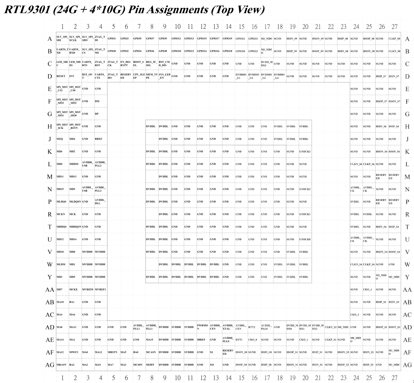
Pin Assignment
The following pinout is the RTL9301, but it's expected considering the identical chip dimensions that the pinout is identical for all 930x.
| Ball | Mux 0 | Mux 1 | |
|---|---|---|---|
| A | |||
| A1 | SPI_SLV_SDI | ||
| A2 | SPI_SLV_SCLK | ||
| A3 | SPI_SLV_SDO | ||
| A4 | JTAG_TDI | UART1_RXD | |
| A5 | GPIO01 | EXT_GPIO_MDC | |
| A6 | GPIO03 | SPI_SCK | |
| A7 | GPIO05 | SPI_MOSI | |
| A8 | GPIO07 | SPI_CS0 | |
| A9 | GPIO09 | I2C_SDA0 | |
| A10 | GPIO11 | I2C_SDA2 | |
| A11 | GPIO13 | I2C_SDA4 | |
| A12 | GPIO15 | I2C_SDA6 | |
| A13 | GPIO17 | I2C_CLK1 | |
| A14 | GPIO19 | LED Sync | |
| A15 | GPIO21 | EXT_MDX_MDC | |
| A16 | GPIO23 | LED_STACK | |
| A17 | M3_MDC | ||
| B | |||
| B1 | UART0_TXD | ||
| B2 | UART0_RXD | ||
| B3 | SPI_SLV_CS | ||
| B4 | JTAG_TMS | UART1_RTS | |
| B5 | GPIO00 | SYS_LED | |
| B6 | GPIO02 | EXT_GPIO_MDIO | |
| B7 | GPIO04 | SPI_MISO | |
| B8 | GPIO06 | SPI_CS1 | |
| B9 | GPIO08 | I2C_CLK0 | |
| B10 | GPIO10 | I2C_SDA1 | |
| B11 | GPIO12 | I2C_SDA3 | |
| B12 | GPIO14 | I2C_SDA5 | |
| B13 | GPIO16 | I2C_SDA7 | |
| B14 | GPIO18 | USB LED | |
| B15 | GPIO20 | ||
| B16 | GPIO22 | EXT_MDX_MDIO | |
| B17 | M3_MDIO | ||
| C | |||
| C1 | LED_MDC | ||
| C2 | LED_MDIO | ||
| C3 | UART0_RTS | ||
| C4 | JTAG_TRST | ||
| C5 | JTAG_TCK | UART1_CTS | |
| D | |||
| D1 | RESET | ||
| D2 | INT | ||
| D3 | RST_OUT | ||
| D4 | UART0_CTS | ||
| D5 | JTAG_TDO | UART1_TXD | |
| E | |||
| E1 | QSPI_NOR_CS1 | ||
| E2 | QSPI_NOR_CS0 | ||
| F | |||
| F1 | QSPI_NOR_SIO3 | ||
| F2 | QSPI_NOR_SIO2 | ||
| F4 | USB_DM | ||
| G | |||
| G1 | QSPI_NOR_SIO1 | ||
| G2 | QSPI_NOR_SIO0 | ||
| G4 | USB_DP | ||
| H | |||
| H1 | QSPI_NOR_SCK | ||
| H2 | QSPI_NOR_RSTN | ||
| Y | |||
| Y27 | M2_MDC | ||
| Y26 | M2_MDIO | ||
| AD | |||
| AD23 | M0_MDC | ||
| AE | |||
| AE24 | M0_MDIO | ||
| AF | |||
| AF27 | M1_MDIO | ||
| AG | |||
| AG27 | M1_MDC | ||
Pin Mux
The RTL93xx doesn't have a pin mux in a traditional sense. While previous generations seems to have had it, the rtl930x seems to remove the notion entirely. Instead, control blocks have a (usually) single bit, indicating if a certain pad is to be setup as GPIO in (usually `0b0`, the default) or whatever special function the pad is part of (usually `0b1` to enable the pad as special function).
RTL931x SoCs
The following section describes the Mango, or rtl931x series. A lot of the things are duplicated from the rtl930x however, and thus only differences are explicitly mentioned here. Note though that this all grows organically however.
SoC series with codename "Mango". All SoCs in this series have a 1004Kc MIPS core.
Common features:
- Dual core MIPS InterAptiv @ 1GHz
- 2MB of packet buffer
| Model number | MODEL_NAME_INFO | Ports | Comment |
|---|---|---|---|
| 9311 | 48GE + 6x 10GE | Stackable, L3, 108GBit (marketing, 216Gbit math, 240Gbit max?) switch cap | |
| 9313 | 12x 10Gb | L3 |
Pin Assignment
The following pinout is the RTL9311, but it's expected considering the identical chip dimensions that the pinout is identical for all 931x.
Dedicated pins to serdes, PCIe etc are left out for briefety
| Ball | Mux 0 | Mux 1 |
|---|---|---|
| A | ||
| A19 | MDC_1 | |
| A20 | MDC_0 | |
| A21 | QSPI_SIO1 | |
| A22 | QSPI_SIO2 | |
| A23 | QSPI_CLK | |
| A24 | QSPI_CS0# | |
| A32 | USB_HSDP | |
| B | ||
| B19 | MDIO_1 | |
| B20 | MDIO_0 | |
| B21 | QSPI_SIO0 | |
| B22 | QSPI_SIO3 | |
| B22 | QSPI_RST# | |
| B24 | QSPI_CS1# | |
| B31 | USB_LED | |
| B32 | USB_HSDP | |
| AG | ||
| AG19 | GPIO17 | I2C_SDA2 |
| AG20 | GPIO20 | I2C_SDA5 |
| AG21 | GPIO26 | I2C_SDA11 |
| AG24 | UART1_RTS# | |
| AG25 | UART1_CTS# | |
| AG26 | UART0_RTS# | |
| AH | ||
| AH17 | GPIO27 | |
| AH19 | GPIO16 | I2C_SDA1 |
| AH20 | GPIO19 | I2C_SDA4 |
| AH21 | GPIO25 | I2C_SDA10 |
| AK22 | GPIO12 | SPI_CS1# |
| AH23 | GPIO05 | JTAG_TRST# |
| AH25 | UART1_TXD | |
| AH26 | UART0_CTS# | |
| AJ | ||
| AJ17 | GPIO_31 | LED_SYNC |
| AJ19 | GPIO15 | I2C_SDA0 |
| AJ21 | GPIO24 | I2C_SDA9 |
| AJ23 | GPIO03 | JTAG_TMS |
| AJ25 | UART1_RXD | |
| AK | ||
| AK17 | GPIO28 | |
| AK18 | LED_SDA | LED_MDIO |
| AK19 | GPIO13 | I2C0_SCK |
| AK20 | GPIO18 | I2C_SDA3 |
| AK21 | GPIO23 | I2C_SDA8 |
| AK22 | GPIO11 | SPI_CS0# |
| AK23 | GPIO03 | JTAG_TCK |
| AK24 | GPIO06 | JTAG_TDI |
| AK25 | GPIO00 | SYS_LED |
| AK26 | SPI_SLV_SDO | |
| AL | ||
| AL17 | MDIO_2 | |
| AL19 | GPIO_30 | SC_MDIO |
| AL20 | GPIO14 | I2C1_SCK |
| AL21 | GPIO22 | I2C_SDA7 |
| AL22 | GPIO10 | SPI_MOSI |
| AL23 | GPIO08 | SPI_SCK |
| AL24 | GPIO07 | JTAG_TDO |
| AL25 | GPIO02 | GPIO_MDIO |
| AL18 | LED_SCK | LED_MDC |
| AL26 | PSI_SLV_CS# | |
| AM | ||
| AM17 | MDC_2 | |
| AM19 | GPIO_29 | SC_MDC |
| AM21 | GPIO21 | I2C_SDA6 |
| AM23 | GPIO09 | SPI_MISO |
| AM25 | GPIO01 | GPIO_MDC |
| AM27 | SPI_SLV_SDI | I2C_SLV_SDA |
| AM28 | SPI_SLV_SCLK | I2C_SLV_SCK |
| AM29 | UART0_RXD | |
| AM30 | UART0_TXD | |
Clock tree
Interrupt Map
Interrupts are a bit more complex with both an interrupt and a routing component. See SoC interrupt controller for details.
| Interrupt source | IRQ | VPE0 IRQ destination (SDK) | VPE1 IRQ destination (SDK) | Notes |
|---|---|---|---|---|
| TIMER0 | 0 | |||
| TIMER1 | 1 | |||
| TIMER2 | 2 | |||
| TIMER3 | 3 | |||
| TIMER4 | 4 | |||
| TIMER5 | 5 | |||
| TIMER6 | 6 | |||
| Reserved for TC7 | 7 | |||
| WDT_IP1 | 8 | |||
| WDT_IP2 | 9 | |||
| Reserved | 10 | |||
| RXI-300 | 11 | |||
| Reserved | 12 | |||
| Reserved | 13 | |||
| Reserved | 14 | |||
| SWCore | 15 | |||
| NIC | 16 | |||
| Reserved | 17 | |||
| Reserved | 18 | |||
| Reserved | 19 | |||
| GPIO0 (ABCD) | 20 | |||
| Reserved | 21 | |||
| UART0 | 22 | |||
| UART1 | 23 | |||
| Reserved | 24 | |||
| Reserved | 25 | |||
| Reserved for TC2_DELAY | 26 | |||
| Reserved for TC3_DELAY | 27 | |||
| TC4_DELAY | 28 | |||
| TC5_DELAY | 28 | |||
| TC6_DELAY | 30 | |||
| Reserved for TC7_DELAY | 31 | |||
| LXSTO | 32 | |||
| LXMTO | 33 | |||
| Lexra Bus Traffic Generator/GDMA | 34 | |||
| Reserved | 35 | |||
| USB_H2 | 36 | |||
| SPI_NAND | 37 | |||
| ECC | 38 | |||
| Reserved | 39 | |||
| Reserved for IPI | 40-47 | Used by MIPS InterAptive Inter Processor Interrupts |
SerDes Port Mappings
Configuration tables for 0x13bc (2 different views)
| SerDes | config 0 | config 1 | config 2 | |
|---|---|---|---|---|
| 0 | 0 - 3 | config 1 only on chan 0 - 3 | ||
| 1 | 4 - 7 | config 1 only on chan 0 - 3 | ||
| 2 | 0 - 7 | 8 - 11 | 4 - 5 | config 2 only on chan 2 + 3 |
| 3 | 8 - 15 | 12 - 15 | 12 - 13 | config 2 only on chan 2 + 3 |
| 4 | 20 - 21 | 20 - 21 | config 0 only on chan 4 + 5, config 1 only on chan 2 + 3 | |
| 5 | 28 - 29 | 28 - 29 | config 0 only on chan 4 + 5, config 1 only on chan 2 + 3 | |
| 6 | 36 | 36 | config 0 only on chan 4, config 1 only on chan 0 | |
| 7 | 42 - 47 | 44 - 45 | config 0 only on chan 2 - 7, config 1 only on chan 2 + 3 | |
| 8 | 50 | config 1 only on chan 2 | ||
| 9 | 50 | 42, 43, 46, 47 | config 1 only on chan 0 - 3 |
| SerDes | conf | ch0 | ch1 | ch2 | ch3 | ch4 | ch5 | ch6 | ch7 | |
|---|---|---|---|---|---|---|---|---|---|---|
| 0 | 0 | 0 | 1 | 2 | 3 | |||||
| 1 | 0 | 4 | 5 | 6 | 7 | |||||
| 2 | 0 | 0 | 1 | 2 | 3 | 4 | 5 | 6 | 7 | |
| 2 | 1 | 8 | 9 | 10 | 11 | |||||
| 2 | 2 | 4 | 5 | |||||||
| 3 | 0 | 8 | 9 | 10 | 11 | 12 | 13 | 14 | 15 | |
| 3 | 1 | 12 | 13 | 14 | 15 | |||||
| 3 | 2 | 12 | 13 | |||||||
| 4 | 0 | 20 | 21 | |||||||
| 4 | 1 | 20 | 21 | |||||||
| 5 | 0 | 28 | 29 | |||||||
| 5 | 1 | 28 | 29 | |||||||
| 6 | 0 | 36 | ||||||||
| 6 | 1 | 36 | Very odd to see port 36 lonely on serdes 9 chan 0 | |||||||
| 7 | 0 | 42 | 43 | 44 | 45 | 46 | 47 | |||
| 7 | 1 | 44 | 45 | |||||||
| 8 | 1 | 50 | ||||||||
| 9 | 0 | 50 | Very odd to see port 50 lonely on serdes 9 chan 0 | |||||||
| 9 | 1 | 42 | 43 | 46 | 47 |
Why are there ports missing?
| Port | opt0 | opt1 | opt2 | notes |
|---|---|---|---|---|
| 0 | 9-0 | |||
| 1 | 2-1 | |||
| 2 | 2-2 | |||
| 3 | 2-3 | |||
| 4 | 2-2 | |||
| 5 | 2-3 | |||
| 6 | ||||
| 7 | ||||
| 8 | 2-0 | 3-0 | ||
| 9 | 2-1 | 3-1 | ||
| 10 | 2-2 | |||
| 11 | 2-3 | |||
| 12 | 3-0 | |||
| 13 | 3-1 | |||
| 14 | 3-2 | |||
| 15 | 3-3 | |||
| 18 | 4-2 | |||
| 19 | 4-3 | |||
| 20 | 4-2 | |||
| 21 | 4-3 | |||
| 26 | 5-2 | |||
| 27 | 5-3 | |||
| 28 | 5-2 | |||
| 29 | 5-3 | |||
| 34 | 6-2 | |||
| 35 | 6-3 | |||
| 36 | 6-2 | |||
| 37 | 6-3 | |||
| 42 | 9-0 | |||
| 43 | 7-3 | |||
| 44 | 7-2 | |||
| 45 | 7-3 | |||
| 50 | 9-0 |